MicroFab: Microfabrication through Electrodeposition
This is a trip report of a visit I made in September 1998 to John
Madden at MIT to work on the microfabrication technique which he describes
in his patent
with Prof. Ian Hunter.
The goal of the two week stay was to duplicate the results described in
the patent, develop some improved control software for running the experiment
and try to improve the control of deposition, especially along horizontal
surfaces.
Update 7/1/99: The Information Sciences Institute at USC has independently
developed a rapid microfabrication technique also using electrodeposition.
See EFAB.
Experimental Setup
The general approach is to use a fine-tipped probe in an electroplating
solution to locally electrodeposit metals out of the solution to form microstructures.
We used 4.7 volts to deposit nickel out of a nickel sulfamate solution
onto a copper surface (or other parts of the previously-deposited nickel
structure).
Below is a diagram of the setup we used, followed by details on each
of the components.
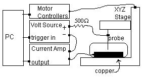
microfabrication setup
-
PC Computer: Windows 95 with a National Instruments PCI-MIO-16XE-10
I/O board ($1995). This is an internal PCI board which connects to an external
BNC-2080 breakout board ($340) with screw terminal connections. We use
one A/D input (-10V to 10V range) and an 8 bit digital output.
-
Motor Controllers: One Compumotor
LN Drive for each of the XYZ axes ($1680 each). Each controller is
set up for 100,000 steps per revolution. Each controller takes three digital
inputs: step pulse, counter-clockwise select, and standby. (One digital
output from the PC controls the standby for all three motors, so the total
digital outputs used is 2*3+1=7 .)
-
XYZ Stage: Three-axis stage from New
England Affiliated Technologies with one CompumotorLN57-51-MO
microstepping motor per axis ($127 each).
-
Voltage Source: HP 3245A universal
source ($5050). This is programmed to cycle through three different voltages
(0V, 1V, 4.7V) based on the trigger input from the PC. (The trigger uses
the eighth digital output from the PC.)
-
Current Amplifier: Keithley
428 ($3390). This has a voltage output, converting one milliamp in
to one volt out. Its range is -10mA to 10mA (-10V to 10V output, which
also corresponds to the A/D range).
-
500 Ohm Resistor: The maximum voltage is 4.7V. The current amplifier
has a limit of 10mA, so a 500 ohm current-limiting resistor limits the
current to 9.4 mA.
-
Probe: 35/25/Epoxy Insulated 30M, catalog #30-10-119721D from FHC,
Brunswick, ME, 207/666-8190. ($87 for 3 probes.) The probe is epoxy insulated
up to the tip. Epoxy worked better than glass which seemed to chip quite
easily slowly exposing more of the tip. The epoxy would fray at the tip
a little bit, but did not seem to slowly keep retreating through use like
the glass.
-
Copper: We actually used the connector sawed off from an ISA board.
It was easy to solder a wire to the connector lead off one of the connector
contacts. The solder joint is covered with protective tape before putting
it in the nickel sulfamate. The copper is inside a dish which can be filled
with the nickel sulfamate. Actually, since the work area is quite small,
we found that it is enough just do use a syringe to deposit a large droplet
onto the copper surface surrounding the probe. It forms a meniscus and
clings to the probe. Therefore we didn't have to fill and empty the dish
every time.
A note on pricing
The prices included above are for the setup we used, but some of the equipment
is clearly overkill. For example, a fully-featured HP 3245A universal source
is certainly not necessary to output 1V and 4.7V. Instead, a buffered output
from the existing D/A board might work as a much less expensive alternative.
Likewise, instead of the Keithley 428 current amplifier, it might be possible
to monitor the voltage across the 500 ohm resistor as a current sensor,
although we haven't tested this. A less expensive second-hand XYZ stage
may be available from ServoSystems.
Of course, a killer app of this fabrication technique would be to manufacture
an adequate stage for the process itself.
Procedure
I will describe the procedure by describing the software which implements
the depositing algorithms. John Madden's lab was already set up to use
Symantec's
Visual Cafe Java development environment, so I continued with its use
to write the control software which is an applet called MicroFab. Below
is a screen shot. Included is a zip file with
all the code, except that the file RealTime.java links to native code in
rtlib.cpp and other files supplied by the I/O board manufacturer which
I could not include.
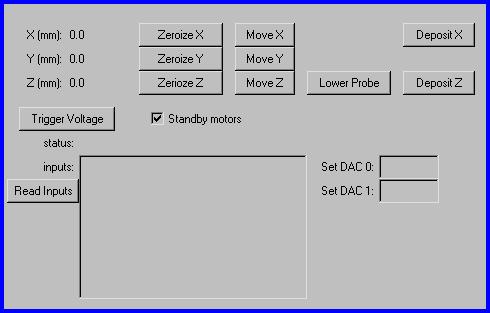
MicroFab main screen
In the upper-left of the screen are readouts of the present position
of the probe on the XYZ stage. Next to the readouts are buttons to zeroize
these readouts to give a new origin for any of the axes. The MoveX, Move
Y and MoveZ buttons simply position the probe without any feedback. (After
you press the button, MicroFab shows a dialog box where you specify how
far to move the probe.) The Trigger Voltage button simply sends a pulse
to the volage source to trigger it to its next value as it cycles through
0V, 1V and 4.7V. And the Standby Motors checkbox turns on and off standby
for all three motors. (In standby, the motors are not powered and the shafts
can be manually turned. With standby off, the motors are activated and
shafts locked.) Set DAC 0 and Set DAC 1 are for testing the D/A outputs
(not used in the present setup) and the Read Inputs button displays the
values of all A/D converters in the "inputs" box.
The real action is in the three buttons on the upper right as described
below.
Lower Probe
To lower the probe, the MicroFab software sets the probe voltage to 1V.
Repeatedly it lowers the probe in the Z direction by one motor step and
reads the probe current. (One motor step results in 0.02 microns probe
movement.) One volt is below the threshold for depositing, so it is only
a test voltage. If the current jumps above a threshold (0.01 milliamps)
then the probe has contacted the surface and MicroFab stops lowering and
sets the voltage back to zero. One detail: while preparing to lower, after
setting the voltage to 1V, MicroFab waits one second before lowering because
there may be some initial capacitive current as the probe charges up.
Deposit Z
Depositing a vertical column in the Z direction is the first operation
we tried, and it worked well on the first attempt. I found it easy to get
repeated results. To deposit in the Z direction, the MicroFab software
sets the probe voltage to 4.7 volts. It repeatedly reads the probe current.
When the probe current is above a threshold of 2.5 milliamps, this means
the probe is close to the growing column of nickel and moves the probe
up one motor step (0.02 microns). If the probe current is below the threshold,
MicroFab maintains the probe position while the nickel column is presumably
growing up to meet the probe. If MicroFab waits for one minute without
reaching the current threshold, it quits. Under normal circumstances it
never reaches this timeout, but when experimenting with different deposit
rates by setting different voltages or current thresholds, it may time
out. This process continues until a column of desired height is deposited.
With the caveat that I could not get an SEM micrograph, just looking through
an optical microscope, I estimate that with the probe specified above the
column is about 20 microns wide. (With a more finely-tipped probe, this
would be thinner.)
Due to the hardware, the speed of depositing is limited to how fast
it can read the I/O board to sample the probe current. Empirically, I measured
one A/D read per 0.3 milliseconds, which includes communication with the
I/O board. At 0.02 microns per motor step, this is a maximum of 66 microns
per second. A normal rate for nickel depositing process is around 10 microns
per second, so the control software is faster than the process, though
not by much. If this becomes a problem (which it was not for us), then
MicroFab can step the motor by a few steps between reading the A/D without
affecting the smoothness of the deposit. Alternatively, we can use a faster
A/D.
Deposit X
Before describing the algorithms we tried for depositing in the X direction
along a surface, which met with some difficulty, I should point out that
we did have success in depositing horizontally "up in the air" as long
as the probe was not in danger of hitting a surface. For example, I made
an inverted L by depositing a column vertically, and then using the same
algorithm as Deposit Z, but moving the probe horizontally off the tip of
the column. Likewise, I deposited a vertical column, and then moved the
probe horizontally in the X and Y directions to draw out the letter Z.
These are simple uses of the same algorithm as Deposit Z.
However, there is a difficulty in depositing along a surface because
the probe can get caught. When MicroFab uses the "Deposit Z" algorithm,
it sets the voltage to 4.7 volts and checks the current. If the current
is above the threshold, then it moves the probe by one step. (In this case
it would be in the X direction along the surface.) But if the probe is
caught on a bump on the surface, it will be contacting and the current
will certainly be above the threshold. So MicroFab will mistakenly step
the motor. As the probe remains caught, MicroFab will step the motor quickly
until it thinks the desired amount has been deposited, but none really
has.
To get around this, we first tried holding the probe several tip diameters
above the surface at 4.7 volts and just scanning back and forth. But there
is a problem of positive feedback here. If a bump on the surface is slightly
higher, the electric field will be stronger and more metal will be deposited
here. That makes it higher and the electric field even stronger compared
to the rest, causing it to grow even more on the next scan. When I looked
at the result, instead of an even deposit underneath the scanning area,
there was one poorly-formed column that reached up to the height of the
scanning probe tip.
A different way to address the problem of the probe getting caught while
depositing along a surface is to make the probe "hop." This is presently
implemented by the MicroFab Deposix X button as follows. MicroFab lowers
the probe to the surface then deposits a column to a height of 0.1 microns
using the Deposit Z algorithm. Then it turns off the voltage, lifts the
probe 25 microns and moves it horizontally 25 microns. The process is repeated,
lowering the probe to the surface, depositing to a height of 0.1 microns
and hopping 25 microns. Once the first layer of the desired horizontal
length is complete (such as 250 microns), MicroFab moves back to the original
location and repeats the process, this time depositing vertically each
time to a height of 0.2 microns above the surface. This is repeated layer
by layer up to the desired total height.
The results were not as expected. Looking in the optical microscope,
instead of a continuous wall, I typically saw a row of columns spaced 50
microns apart, with each column of the desired total height. A likely explanation
is that MicroFab properly deposits the first column up to the height of
0.1 microns, lifts the probe 25 microns and moves horizontally 25 microns.
But when it goes to lower the probe to the surface, the probe encounters
an electrical contact before it fully reaches the surface, due to some
stray material hanging off the previous column, or because the probe may
be too fat. Since after "lowering", the probe is above 0.1 microns and
in electrical contact, MicroFab does not do any vertical deposit, but raises
the probe 25 microns and moves horizontally again 25 microns. This time
MicroFab successfully lowers the probe to the surface, now 50 microns away
from the original column. Thus it skips every other 25 micron site.
Future Work
Although we could not get reliable results with the Deposit X algorithm,
I should mention that during one trial I did see a fairly continuous wall
as expected. So this suggests that under the right circumstances the procedure
can work. But I could not repeat this result. For future experiments, I
would like to try the following:
-
In the Deposit X algorithm, after lowering the probe to the supposed surface
and getting electrical contact, as long as the probe is near the proper
height, MicroFab should apply the voltage for a period anyway, even though
it will be above the current threshold. This may prevent it from skipping
every other column and "fill in" the wall more.
-
The probe we used may have simply been too fat. A sharper probe may allow
the algorithm to work better.
-
For horizontal depositing, try angling the probe 45 degrees and using an
algorithm more like the original Deposit Z. In other words, first lower
the probe to the surface, then raise about one tip diameter. Then begin
depositing, moving a step horizontally when probe current is over the threshold.
Since the probe is angled away from the direction of motion, perphaps it
will not get caught on bumps on the surface. Of course, using an angled
probe only allows horizontal depositing in one direction, but with a proper
"raster scan" regime, this may be useful.
-
I did not get an SEM micrograph of the vertical columns, but I suspect
they are not as smooth as we would like. There are a few possibilities
to try: change to a voltage somewhat lower than 4.7 volts, which will yield
a slower but maybe smoother deposit.
-
Also, try a lower current threshold: It may be possible to use a much more
sensitive reading than 2.5 milliamps so that the probe can be moved before
the deposited material fully reaches the probe. The present technique may
be causing the probe wait too long and then move in bursts, resulting in
a less smooth surface.
-
It may be possible to estimate the depositing rate and keep the probe moving
slightly ahead of the growing column, even while the probe current is under
threshold. Again this may smooth out the depositing process.
-
And lastly, there are several other materials besides nickel which can
be deposited, such as other metals, semiconductors and polymers. Most notably,
there may a polymer which conducts during the electrodeposition, but which
can be later immersed in a dopant which would change it to an insulator.
Therefore by alternating between depositing this polymer and nickel, and
later doping the polymer into an insulator, it may be possible to create
structures with electrically isolated regions.
Conclusions
Microfabrication using electrodeposition is an inexpensive process using
simple equipment, low power levels and relatively benign materials such
as nickel sulfamate. I found the process very forgiving, considering that
we were controlling if from a Java application running within Windows 95
(as opposed to dedicated control hardware). Depositing material vertically
and in circumstances where the probe cannot get caught yields repeatable
results. More work needs to be done on depositing material along a surface
where the probe can contact pre-existing material.
Back to Main Page